Some days ago, I receive a Digital Paddle Clock PCB from Dangerous Prototypes. This is a great page to visit, they have a lot of designs and ideas. Also, three days a week, they give some free PCB’s to their readers. After a lot of comments in their page, I finally win a coupon so I can change it for this PCB.
- The Board
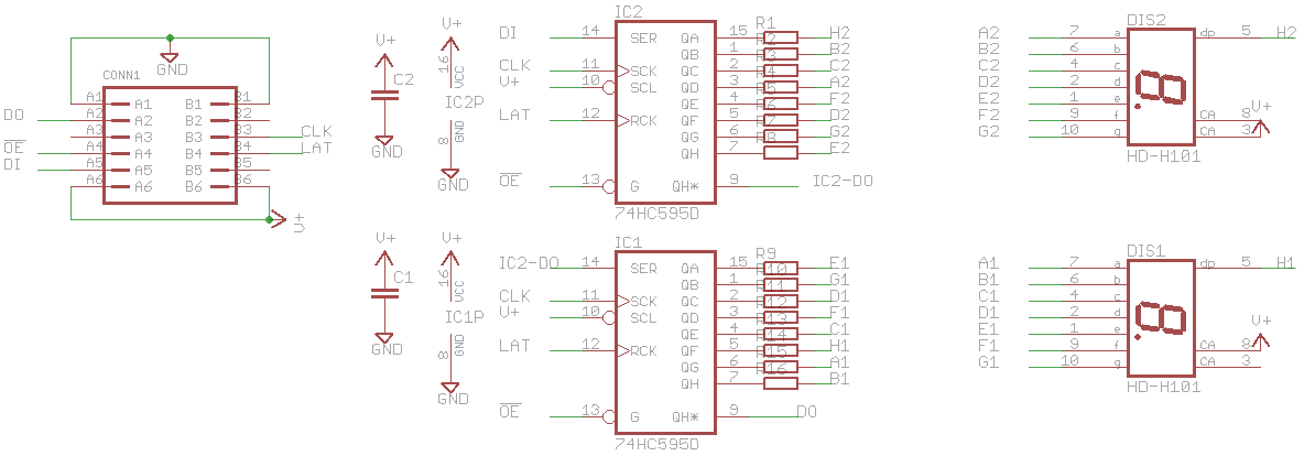
This board is a simple 2-seven segment display, controlled by two 74HC595D shift registers connected in cascade. With this method, you can control up to 16 outputs with only three pins of your favorite microcontroller. Here is the scheme of the board:

Notice that IC2 controls the right display, and IC1 controls the left one. This is important because when you send the data to the displays, the fisrt 8 bits are send is to the left display and the last 8 bits goes to the right one. Also, this board is designed for an anode common displays, so to turn on each segment, you must send it a ‘0’.
- Mounting the board
I mount the board with components that I’ve at home. For this reason, I mounted equivalent components in the case of the resistors and displays. I use these components:
– Display: Kingbright KCSA56-105. These are SMD displays, and fits very tight in the PCB footprint, but it works ok. One note: the left one is mounted 180º of its original position in the PCB (with the dot bottom right, instead of top left), so the conversion table to show the charactes are different for left and right displays.
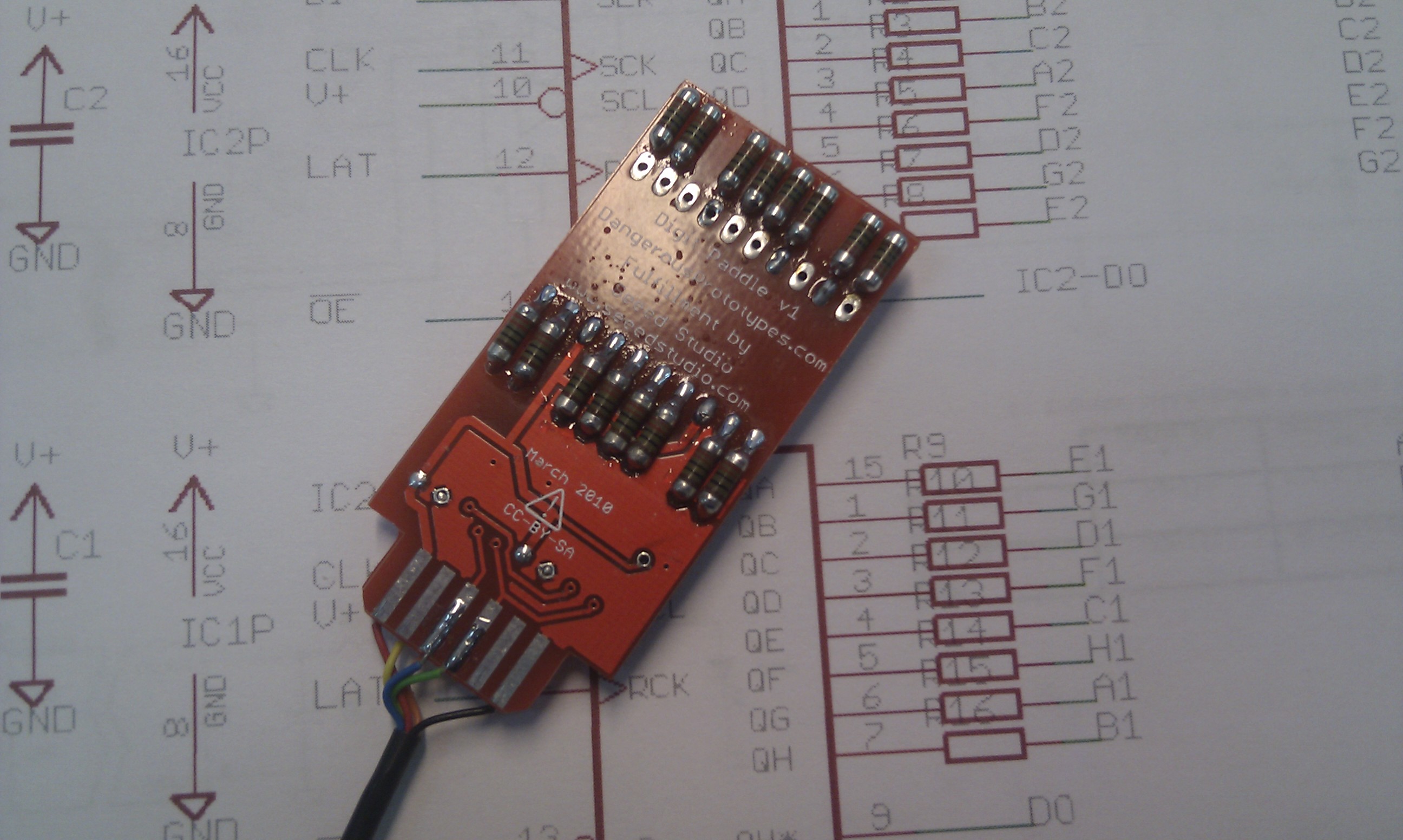
– Resistors: 220 ohms SMD MELF. Again, its fits very tight in the PCB footprint. For this reason, I mounted in the solder layer.
– Capacitors: 100nF SMD 0805.
– Shift Registers: 74HC595D from NXP.
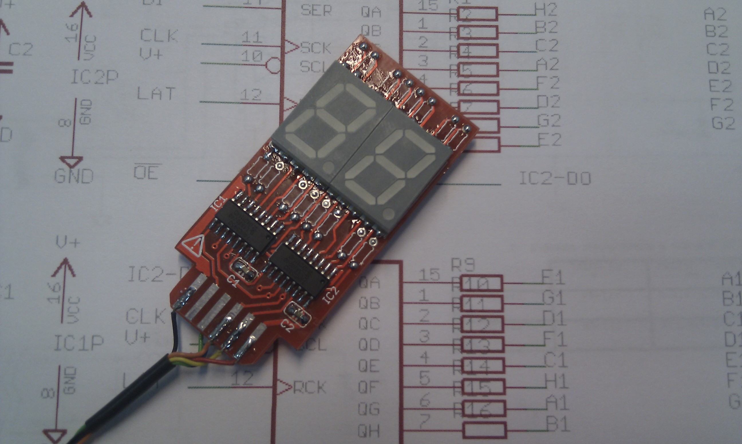
Here’re a couple of photos with all the components:


To interface with the microcontroller, I used these colors:
– Red wire: VCC (+3.3V)
– Black wire: GND
– Orange wire: OE# (Output Enable)
– Yellow wire: DI (Data In, from microcontroller to shift registers)
– Green wire: CLK (Clock to shift data into the registers)
– Blue wire: LAT (Latch signal)
- Software to run it!
To use these breakout board, you need a board with a microcontroller in order to interface it and send the data that you can visualize in the displays. I use my ‘DSETA’ CPU, a board based in a AT89C51RE2 microcontroller, from Atmel. This microcontroller has a 8051 core, with more peripherals, Flash and RAM memory, and can be run at 2x speed that the original 8051. The board has many peripherals, such as:
– USB to serial port bridge, based on the TUSB3410.
– RTC with battery backup.
– Two I2C ADC converters, 8 bits of resolution each.
– Two pushbuttons, two switches, three leds and a buzzer for general purpose.
– External EEPROM, up to 1Mbit capacity (24LC1026 memory from Microchip).
– Temperature sensor (DS18B20 from Maxim Integrated)
– I2C expansion connector (+5V), to connect external devices (such a 2×16 LCD display with an I2C expander)
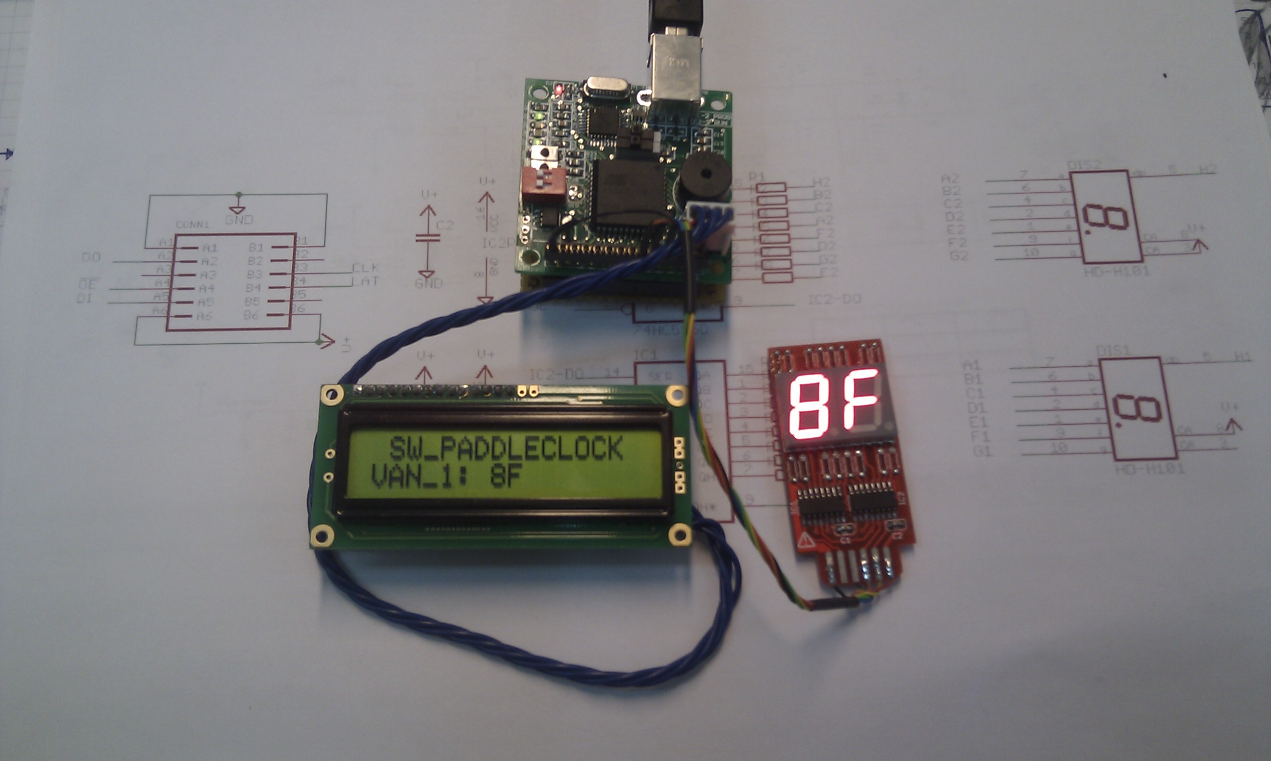
And a few more….maybe another day I’ll write about this board. To test the Digital Paddle Clock, I write a simple program that reads one of the ADC and shows the measure in the displays (0x00 – 0xFF full scale, 8 bits precision). Also, I show the measure in a 2×16 LCD display (connected to the I2C bus with an MCP23017 I2C expander from Microchip) to see that both indicators shows the same measure.
Here are the result:

Measuring 1.85V (full scale is 3.3V)

Full Scale (3.3V). Both displays shows the same measure!!
Also, I use as a 1 second counter to test all the characters. Here you can see it:
Date, time, temperature (ºC), system status and a 1 second counter!!!
From here, I want to thank Ian (Dangerous Prototypes) two things. The first one is, obviously, the board, because I love electronics. It’s my work and my hobby. And the other thing is that with this project , I start a blog, that was one thing I’ve pending for a lot of time. Thanks!!!


Ahaa, its nice conversation regarding this article at this place at this web site,
I have read all that, so now me also commenting here.