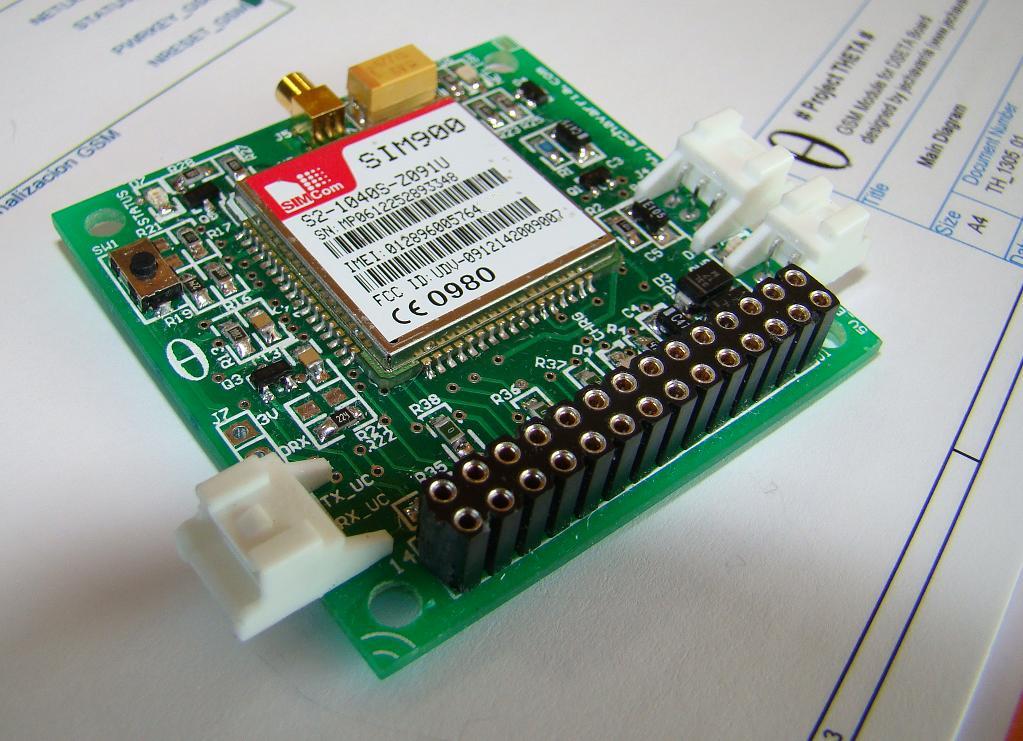
 After some months out, I come back with my last board, the SIM900 Breakout Board. It’s a board based on the popular SIM900 GSM modem, and I design to work with the DSETA board I develop previously. Also, the board can be used without this board, I try to design it in the way that can be used with any microcontroller. From here, I want thanks to Ioannis Kedros from Embedded Day his support in the design of the battery charger, and to Sonia Muñoz, FAE from EBV, a great professional and a better friend, she always helps me when I need. So, let’s go to see what’s inside the board!
- The Hardware
In this post, I only cover the hardware of the board. In an upcoming entry, I’ll develop a full application with this board and I cover the software aspects of the design.
This board is designed to use with a microcontroller-based board. It can be powered from a Li-Ion battery, so includes all the necessary electronic to charge and monitoring the battery. The schematics of the board can be download here. As usually, the schematic is divided in functional blocks, and here’s a brief description of each:
Main Diagram: All the blocks of the system are in this page, including the the relationship between all the signals. Note that with R35-R38, you can isolate the DTR, RI, NETLIGHT and INFO signals from the IO connectors, if you don’t populate.
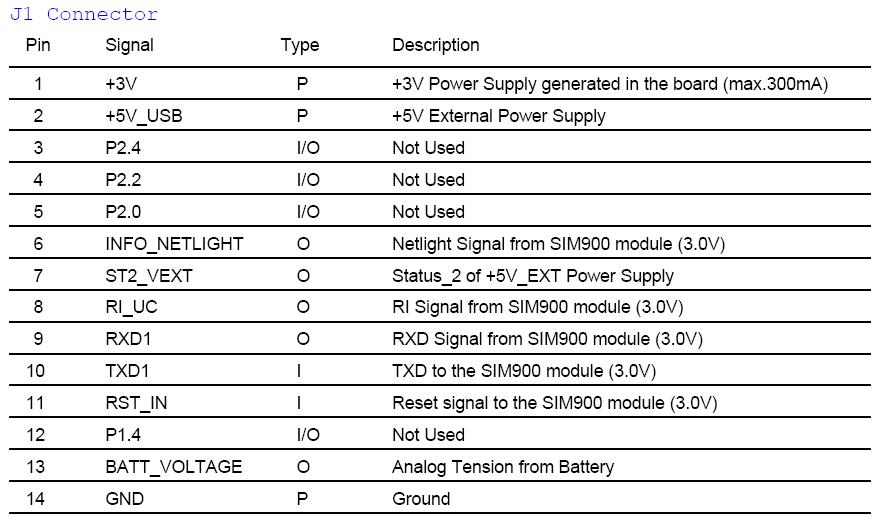
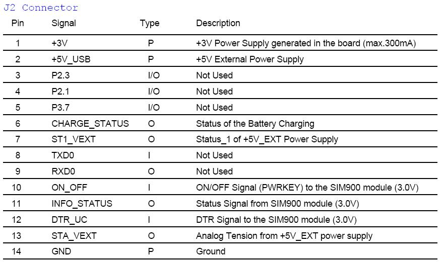
IO Connectors: This are the connection of the board with the rest of the world. It’s design to fit with the DSETA board, but you can use any other board or microcontroller to interface with it. The two connectors has 14 pins and has an standard 100 mils step. Here are the description of each pin of each connector:
Power Supply and Battery Charger: This board can be powered from three different sources:
- Power supply from external +5V (+5V_EXT) using J3 connector.
- Power supply form the IO connectors (+5V_USB), using pins #2 from J1 or J2 connectors.
- Battery supply, using J4 connector.
To allow two external +5V power supplies, I use schottky rectifier diodes from Vishay (SSA33L) to parallelize it. I use this voltage to charge the battery, through the U1. I use the Microchip MCP73832T-2ACI/OT battery charger. This device is a highly advanced linear charge management controller for Li-Ion and Li-Polymer batteries. As the battery has enough current to power the system, I fix the charge current at 100 mA, with a R4 value of 10K. The battery I use to power the system is the LP653450, a 3,7V / 1100mAh Li-Ion battery pack. The standard charging voltage for this battery is 4.2V, so the battery charger model must be fit with this requeriment. From this stage, two signals goes to the IO connectors: CHARGE_STATUS, a digital signal that indicates if the battery is charging (also, led D4 indicates the status visually), and BATT_VOLTAGE, an analog signal to measure the level of the battery. The second part of the schematic corresponds to the LDO regulator. This circuit used the input voltage to obtain the +3.0V necessary for the digital part. So, the microcontroller or board you use with this module must be fit to this voltage. The regulator is the TC1173-3.0VOA from Microchip, that has a maximum dropout of 480mV. This regulator can give an output current of up 300mA, enough to power a board with a microcontroller. This output power supply is available in the IO connectors. And finally, the external +5V_EXT power supply is monitored with three independient circuits. Why? This is for a future application……stay tuned!
SIM900 Module: The heart of the board. There’s a lot of information and breakout boards over the net, I gather info basically from the manufacturer and from here. Some tips about this part of the board:
- C7 and C8 capacitors must be of 470uF or higer. Two capacitors of 100uF can’t absorb the current surges in transmission and reception modes and the module resets. With the highger capacities, this is resolved.
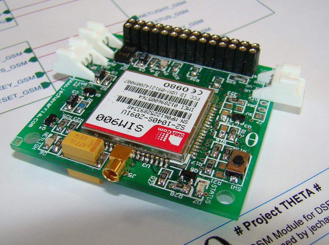
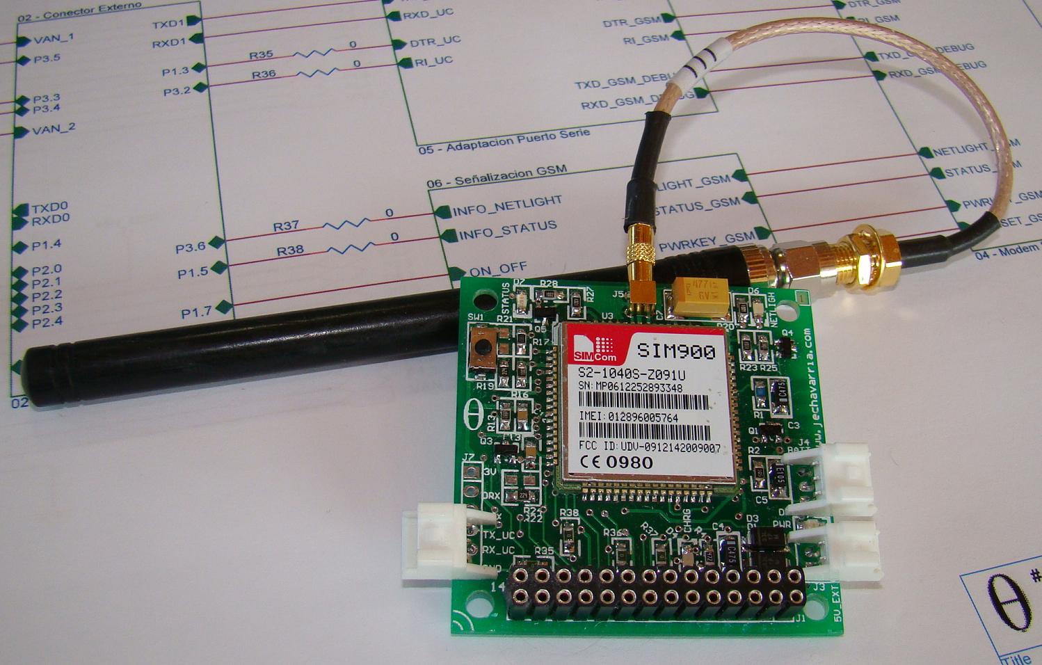
- I use a right angle MMCX connector from Samtec. I want to use a SMA connector, but it’s size is prohibited.
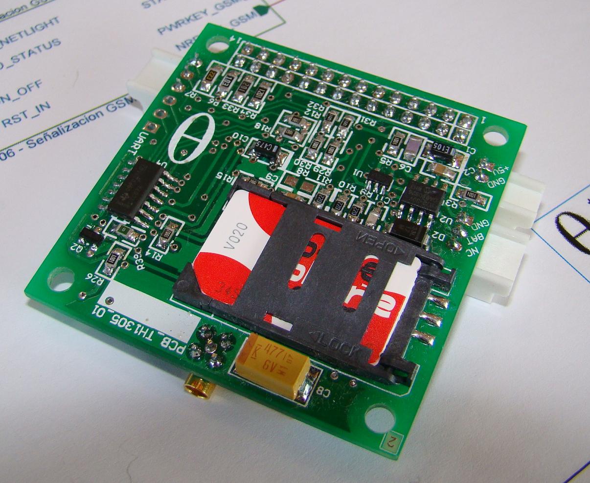
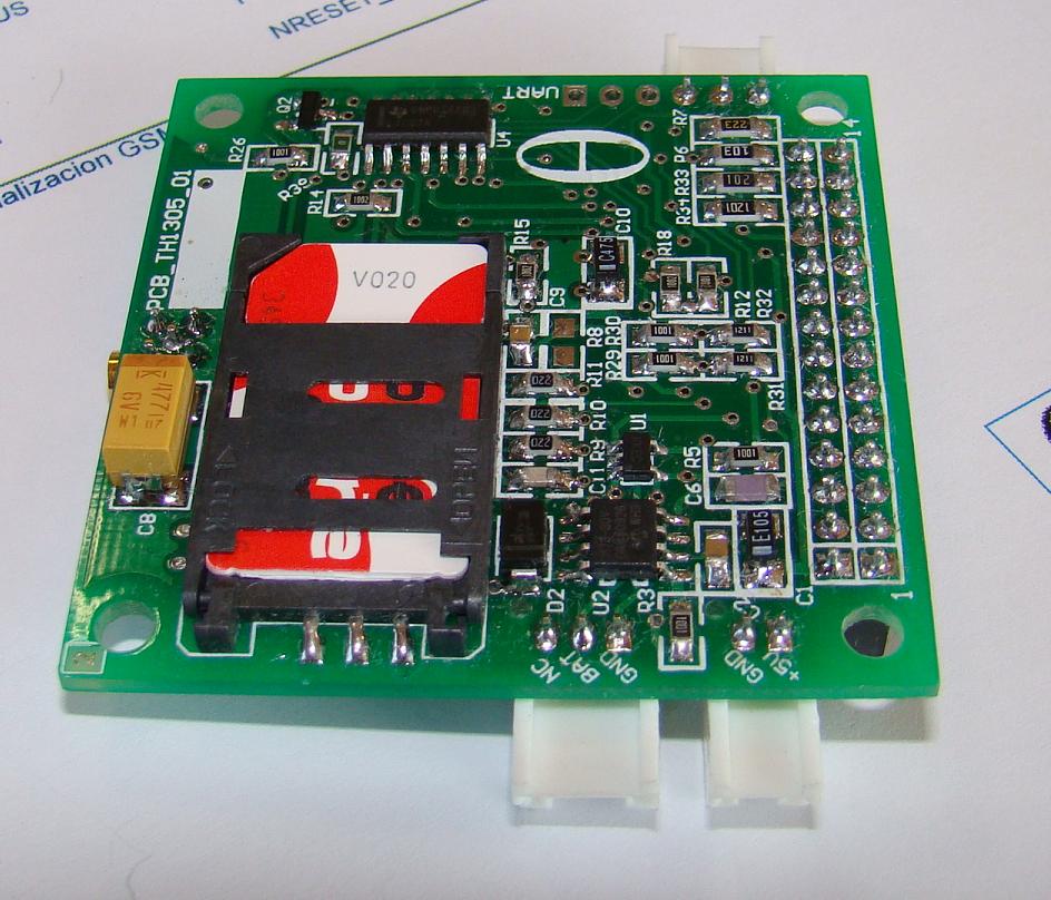
- I found the SIM connector in eBay. The schematic is the recommended in the SIM900 datasheet and works very fine.
- Only TXD_GSM and RXD_GSM signals are necessary to work with the module. However, I also used more signals to work with the module, in the following pages I discuss about it.
Serial Ports: All the serial port signals are adapted from 2.8V (SIM900 output) to the working voltage of 3.0V. To do this adaptation, a SN74LVC07 tri-state buffer is used. To the IO connectors, TXD, RXD, DTR and RI signals are carried. I also carried TXD and RXD debug port to an external connector, J7, for future uses.
SIM900 Signaling: The last page is used from SIM900 status signals. RESET and ON_OFF signals are controlled from the microcontroller, in order to power-up properly the SIM900 module (you can see the power-on and power-off sequences in the datasheet here: SIM900_Hardware_Design_V2.03). NETLIGHT and STATUS signals come from the SIM900 module. and can be used to supervise the status of the module. Both signals are carried to the IO connectors, so the microcontroller can read it. Also, both have a yellow led to visualize it:
NETLIGHT (D6): Network Status:
- Off -> SIM900 is not running.
- 64mS ON / 800mS OFF -> SIM900 not registered on the network
- 64mS ON / 3000mS OFF -> SIM900 registered on the network
- 64mS ON / 300 mS OFF -> GPRS communication established
STATUS (D7): Power On status:
- Off (pin STATUS = 0) -> Module is power down
- On (pin STATUS = 1) -> Module is power up
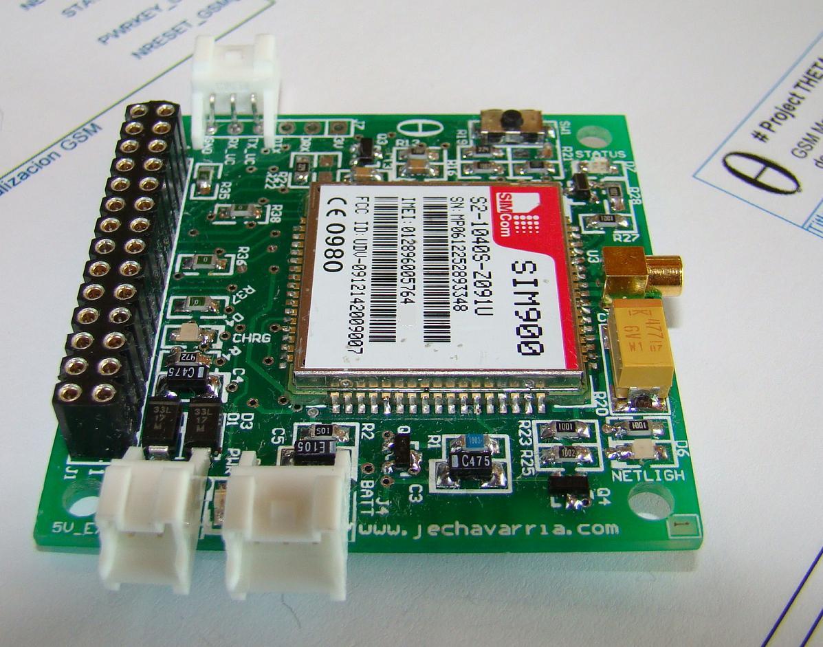
Some photos of the assemble board:
Bottom Layer (Another View)
Top Layer with MMCX to SMA adaptor and Antenna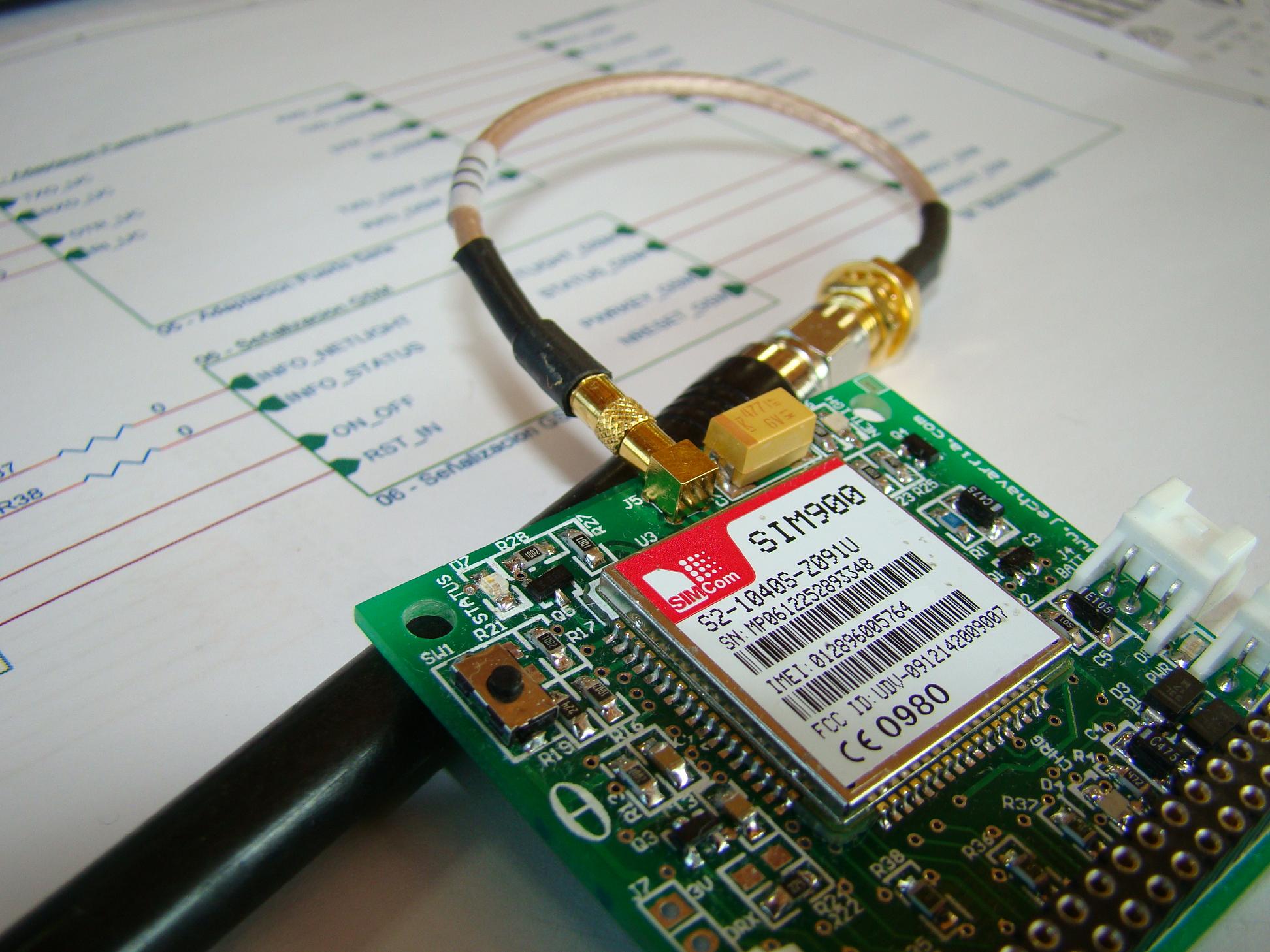
Top Layer with MMCX to SMA adaptor and Antenna (Detail)
- PCB Design and mounting components
I try to perform the design in a 5cm x 5cm board, because I want that this board fits with the DSETA board. Also, I follow the PCB specifications from Dangerous Prototypes, in order to use the DP5050 case also available at Seeedstudio. Another thing that I’ve got in mind is that I’ll mount the board by hand, so size components and distances must be enough to allow the manual mounting. The board is designed using Protel 2.71 and Protel 99SE to generate all the documentation, including gerber files and topographic schemes to placing the components. Again, I use the Seeed Studio PCB Fusion service to order the boards. Now, they’ve the 100%E-Test at free of charge, a great notice because I think it’s a ‘must have’ feature for these kind of boards.
- Integration with DSETA board
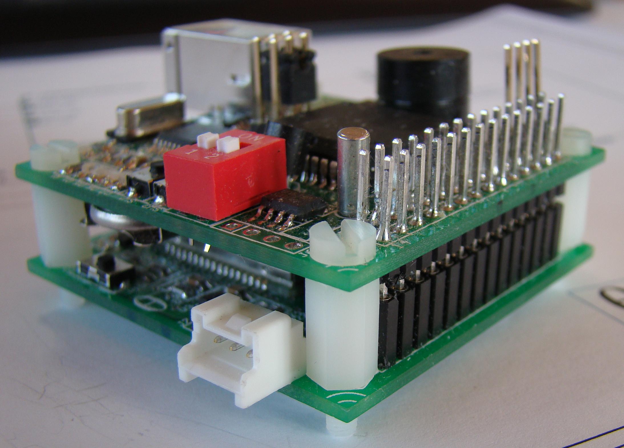
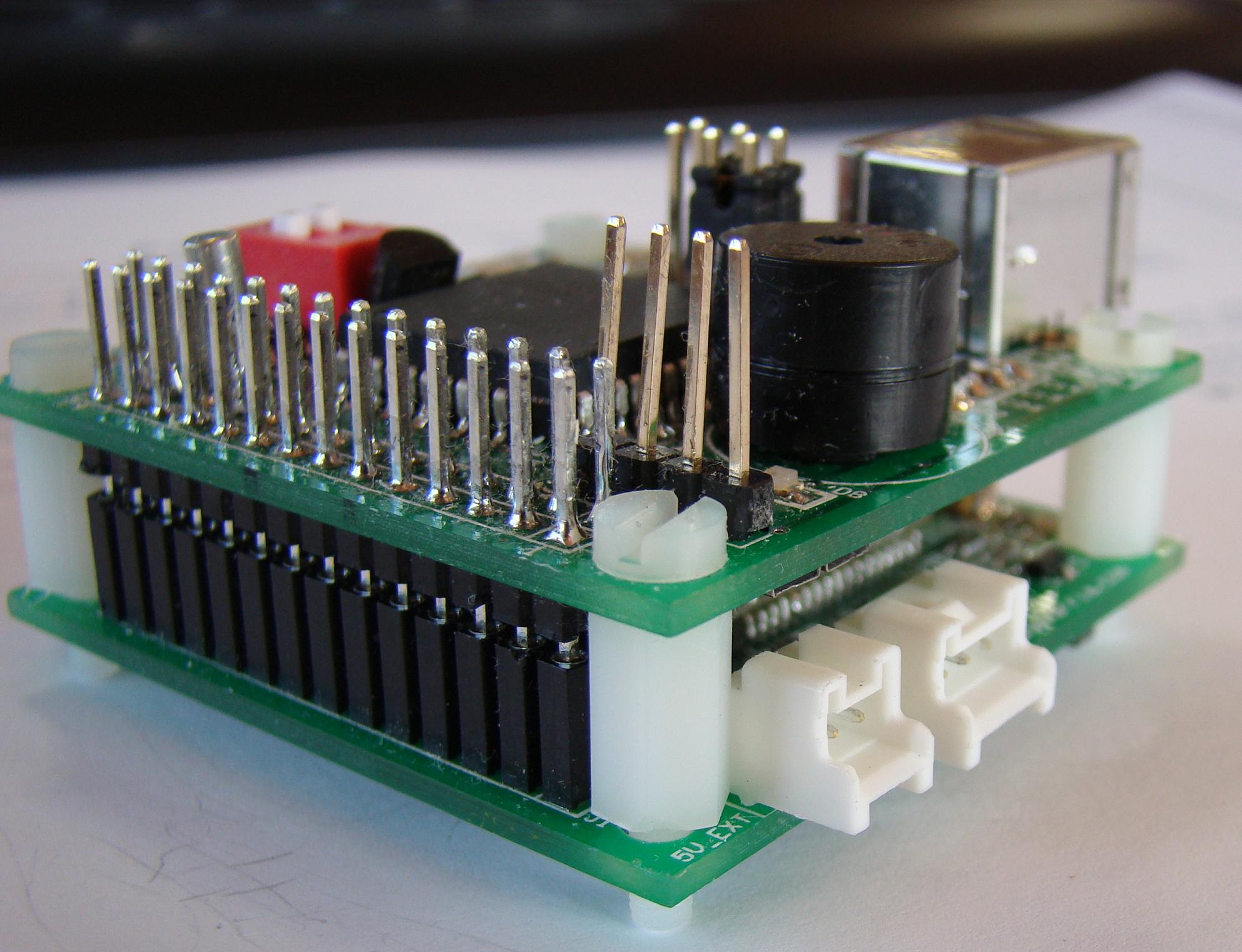
This board is originally designed to use in conjunction with the DSETA board I develop before. So, after assembling the board, the next step is check that the two boards fits well. The result is great, here’re some pics of both boards:

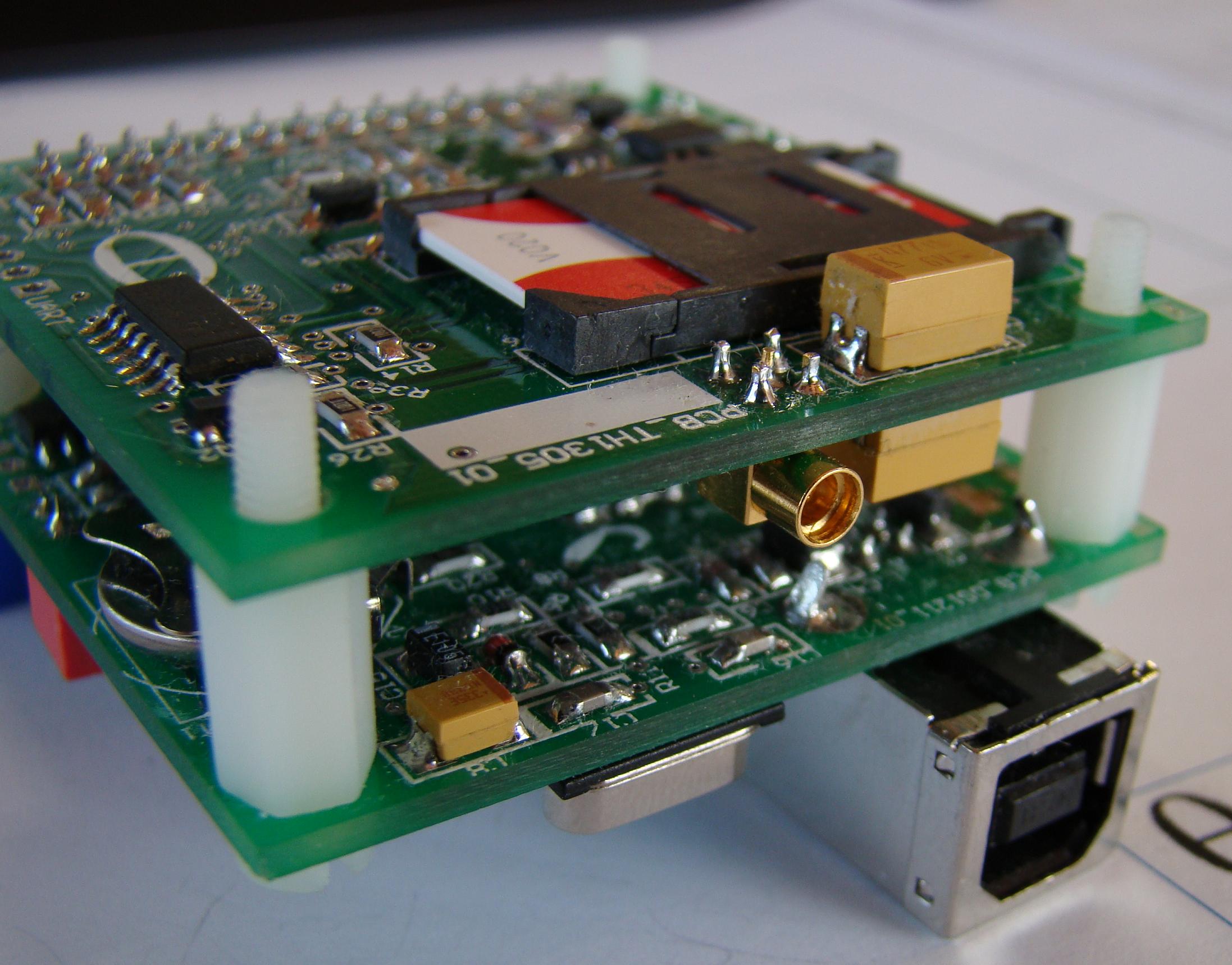
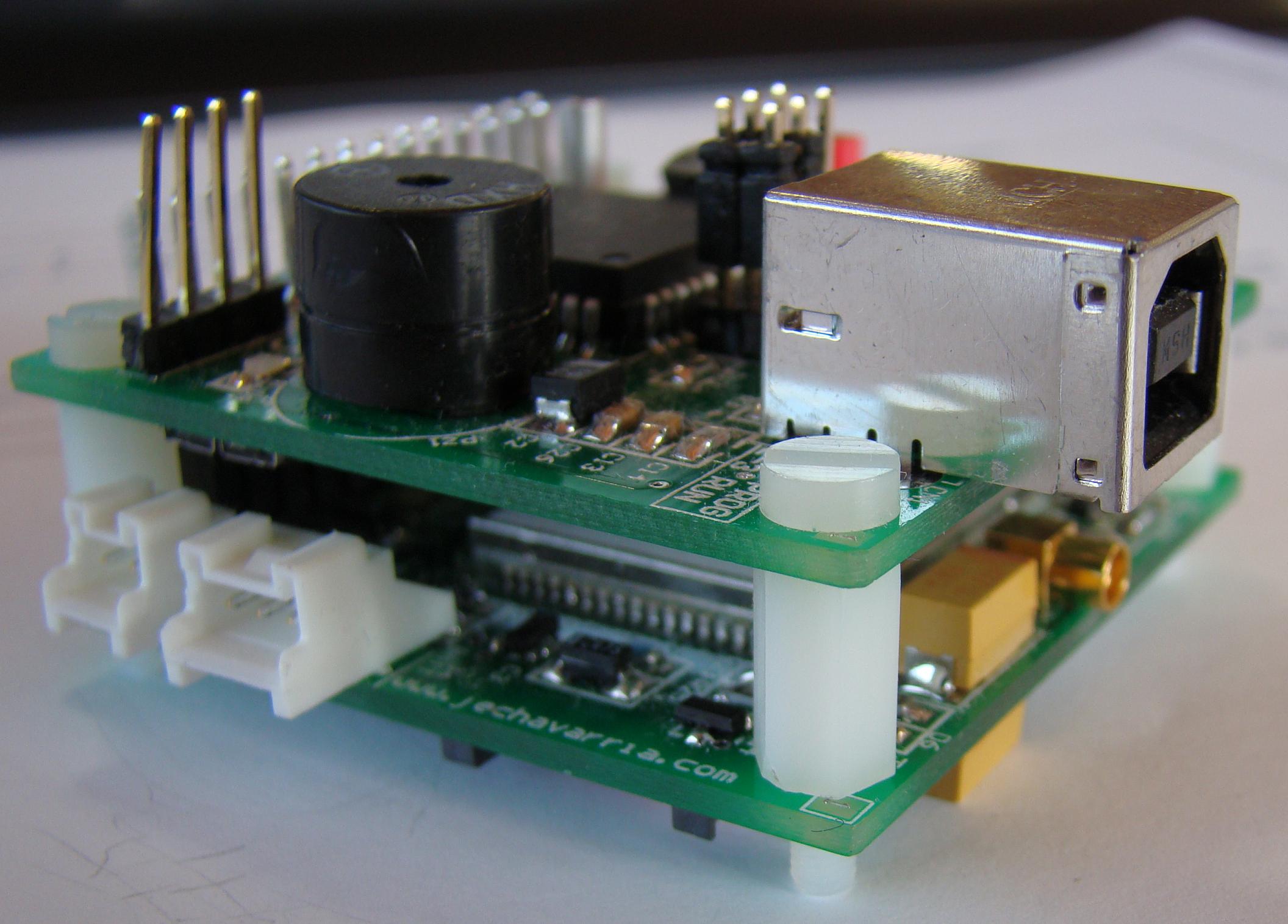
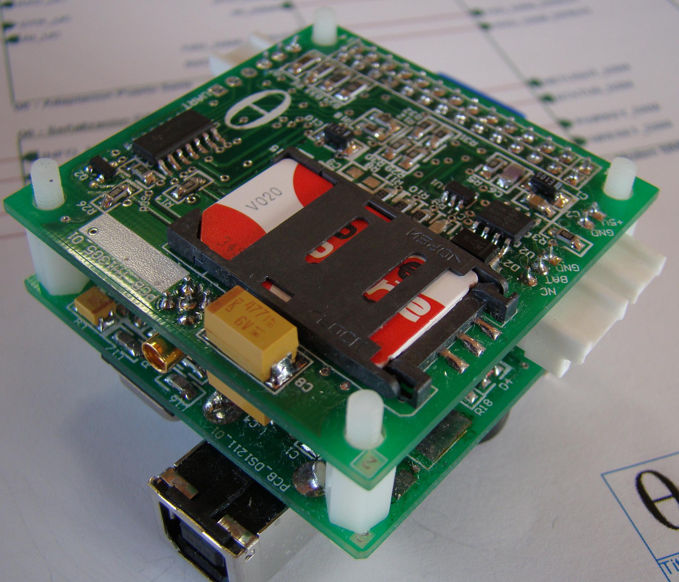
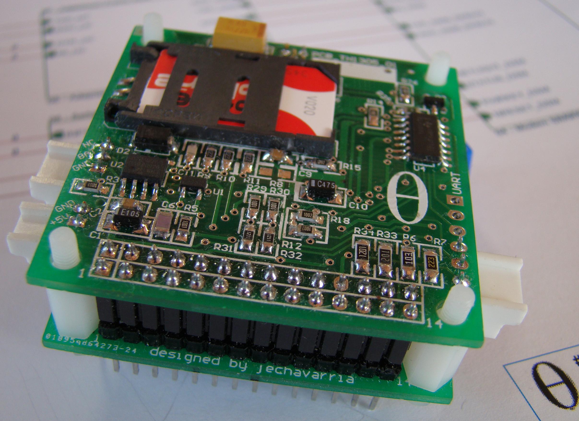
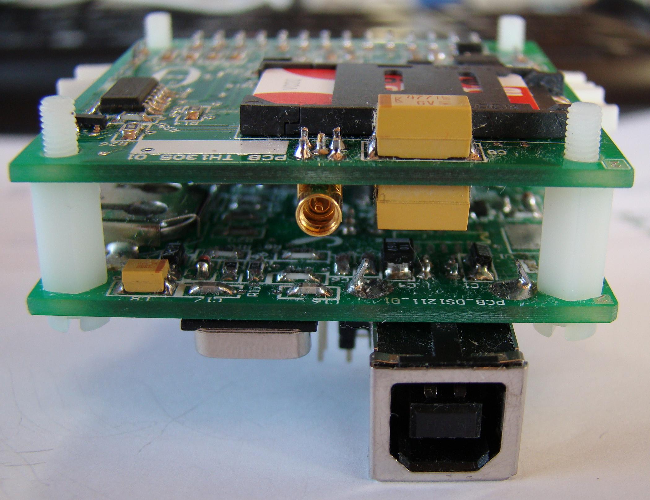 In the next days, I’ll post an entry with an interesting application using these two boards. In this post, I’ll cover all the software aspects related to the communications with the SIM900 module.


I first read about you in DP blog.
Reading you from Spain (Malaga) ;)!! So interesting Blog. Direct way to my feeds reader
Nice project indeed. Just one question. You;re saying that “The battery I use to power the system is the LP653450, a 3,7V / 1100mAh Li-Ion battery pack” and I would like to know if possible the source to purchase them. Also I noticed that the LPxxxxxx seems to be a Li polymer battery code, although the link directing us to Li-ion 3710 battery. Anyway since the charger support both types there should be no problem I guess. However I can’t find the coreect type from any online source, can you point us where to obtain it?
Thank you in advance
Sotris
Thank you for this great project.
Is it possible to order 1 board ready to use ?
Or do you know a seller who can sell to me it ?
Excellent project, thanks very much for sharing !
I noticed that you are using a 10K/23K divider for measuring the battery voltage. For the usable battery voltage range of 3.4-4.2V this gives a 735-908 ADC measurement range (VREF = 3.3V). Note that by using a 10K/33K divider, this voltage range gives a higher 810-1000 ADC range, which means more resolution and lower consumption at the divider (98 uA).
Hi Vassillis!
Thanks for your comment! You’re right, with these resistor values the ADC range will be better. When I continue with the project (I’m very busy now), I’ll test it and share with you the results, but certainly will work better than now. Thanks!!
Hi Jesus,
Nice designs :-). I would like to attempt to build this, slightly altered.
I noticed that R8, R16, R21, and R24 have “nm” as their value.
Could you please let me know what the values of these resistors should be.
Many thanks, Ol.
Hi!
Thanks for your comment. ‘nm’ means ‘not mount’ so these resistors are not used. Good luck with your build, and if I can help you with anything, please tell me!
Regards, Jesus
Great.
Many thanks for the feedback.
And thank you for your offer to assist.
Kind regards,
Ol
Thanks to you. Good luck with your system!!
Pingback: SIM900 USB Communication using MCP2200 -Use Arduino for Projects